Copper CAM software for single layer PCB
Copper CAM software for single layer PCB
video tutorial
Fabrication Process.
Open the software then choose File →Open →New circuit.
Then select “Drill_PTH_Through.DRL” for Drills from the Gerber files which you have generated.
Do not choose anything for Component Side.
After opening the file, it will look like this:
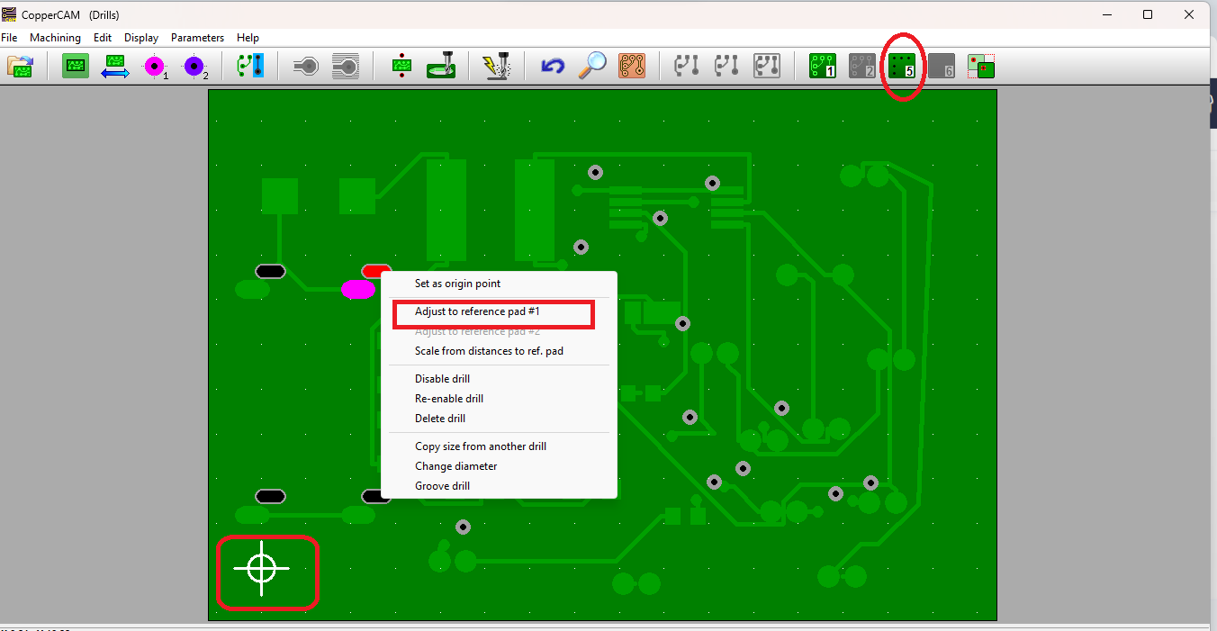
Now if the drill holes are shifted we have to adjust them by selecting the corresponding track footprint of hole after that we have to right click on mouse and select "Set as reference pad "
Now select the drill layer and click the corresponding drill hole and right click on it and select "Adjust to reference pad #1" to match the drill holes.
Note : here origin is not on x= 0 & y= 0 position.
.
Now choose,
File→ Dimensions. Give the values as shown in the figure and choose OK.
A warning dialog box will appear once you choose OK in that select NO option.
Next choose,
File →Origin. Make changes as shown in the figure and choose OK.
Next choose,
Parameters →tool library. Make changes for 0.8 Endmill as shown in figure.
In the same dialog box do changes for 0.2 Conical Engraver as shown in the figure then choose
OK (you can edit the tool parameters here ).
Next choose,
Parameters →Selected tools. Make changes for as shown in figure.
Next choose,
Machining →Card contour Cut whole card (Choose only if cutting layer is not added).
Then go to Calculate contours as shown in the figure.
A set contours dialog box will appear in which specify the values as shown in the figure and
choose Ok. Just after the contours in the right side a hatches option is present which removes the excess
copper in copper clad
.
Now choose,
Machining → Mill then choose the operation and click ok.
Note: never click the mirror option for single layer pcb.

Note: By using 0.2 mm conical engraver we can engrave 0.1 mm of track width and the difference between the two adjacent track must be greater then 0.3 mm.
Related Articles
copper CAM software for double side pcb
Fabrication Process. Open the software then choose File →Open →New circuit (for top layer). Then select the File →Open →Additional layer and add “Gerber_ Bottom Layer .GBL” file for bottom side then add the drill file “Drill PTH Through .DRL” for ...